It’s been nearly 30 years since I managed to pass my Digital Circuits and Microprocessor Design classes. Ah, those were the days! We were so unpolished that, to make our circuits work, we had to stealthily place a finger on the circuit, hoping the assessing professor wouldn’t notice… Obviously, jumping headfirst into software professionally was the sound choice.
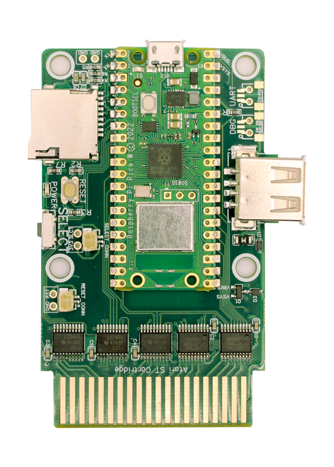
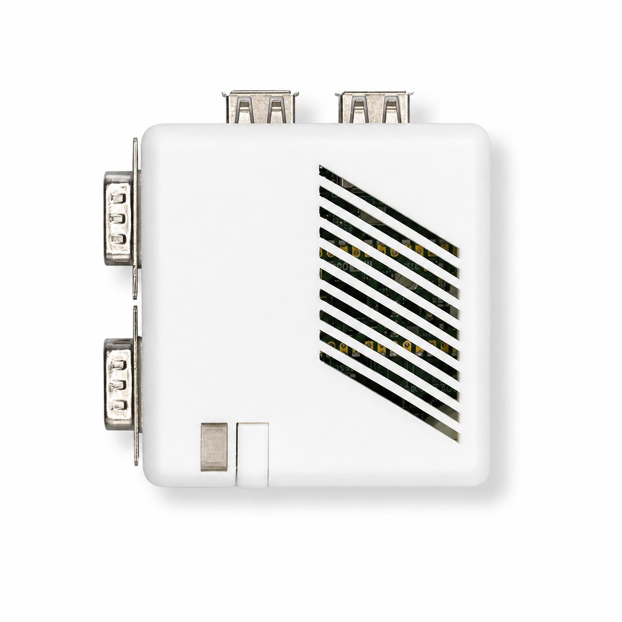
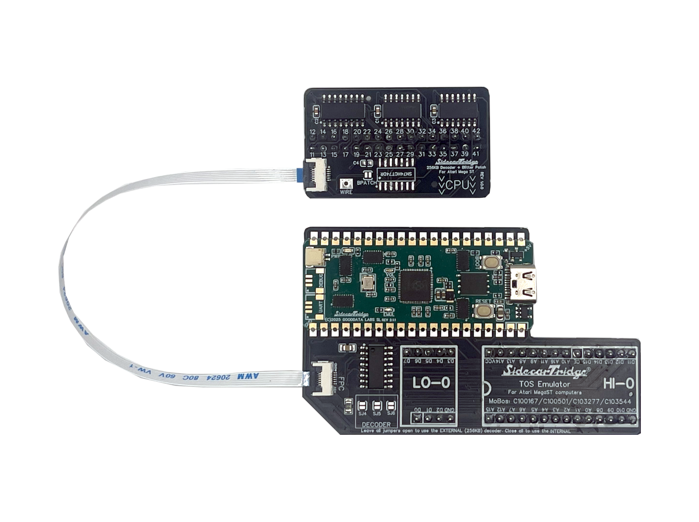
A few months ago, I rolled up my sleeves to create SidecarTridge Multi-device. The first hurdle? Understanding the nooks and crannies of the Atari ST cartridge interface, learning its quirks, and above all, ensuring not to incinerate the circuits of my beloved Atari ST computers.
Overview of the Atari ST Cartridge Interface
The Atari ST, released in the mid-1980s, featured a cartridge port, which was an essential feature on many computers and game consoles of that era.
The Atari ST’s cartridge port was primarily designed for:
-
Software Expansion: Cartridge ports allow software to be loaded instantly, bypassing the need for disk-based loading. This was especially beneficial for some applications and games, offering a quicker and more user-friendly experience.
-
Dongles for Software Protection: Back in the 80s and 90s, software piracy was a significant concern. One way to combat unauthorized copying was the use of dongles — physical hardware devices that plugged into a computer’s port (often a parallel, serial, or cartridge port). Software could check for the presence of the dongle and only run if the correct dongle was present. Some commercial software for the Atari ST used dongles that plugged into the cartridge port as a form of copy protection.
-
Diagnostic Tools: The cartridge interface could be used for hardware diagnostic cartridges. These would boot the system into a diagnostic mode to check the system’s functionality and troubleshoot issues.
-
Hardware Expansion: Beyond its more software-oriented roles, the cartridge interface also opened doors to hardware augmentation. It allowed the connection of additional hardware modules to extend the capabilities and functionalities of the Atari ST, offering a playground for enthusiasts and developers to experiment and innovate.
Diving into the Technical Heart: The Intricacies of Atari ST’s Cartridge Port
The Atari ST’s cartridge port was a direct extension of the system’s bus, reflecting the underlying hardware technology and design principles of the time.
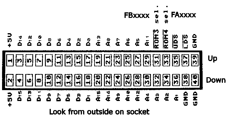
The cartridge port featured a double-row 40-pin configuration designed to directly access the system’s bus. This made the addition of external cartridges straightforward, as they could directly interface with the main system without complex adapters or converters.
The Atari ST, like many computers of its era, was primarily based on TTL (Transistor-Transistor Logic) technology. This means the logic levels (i.e., what’s considered a logical “high” or “low”) were defined by typical TTL voltage levels. In practical terms, a high signal would be close to +5V, and a low signal would be close to 0V. This aspect will be key in the design of SidecarTridge Multi-device, as we will see. The cartridge port provided a +5V power pin to supply power to the cartridges. This was consistent with the TTL logic levels used in the Atari ST. Additionally, ground pins were provided to complete the electrical circuit and ensure proper operation.
The design of the cartridge port had a reduced number of 68000 control lines. This simplification was crucial to ease the construction of cartridges, making it more feasible for developers to create a range of hardware expansions without dealing with excessive complexity in interfacing with the 68000’s control lines. Interestingly, the designers of the Atari ST made a conscious decision for the cartridge port to be read-only. This choice might have stemmed from the simplification of control lines or potentially due to budget constraints; it’s a bit of a mystery. While this read-only nature was a limiting feature for solutions relying on the cartridge, it inevitably sparked the ingenuity to develop smart workarounds.
The Atari ST featured a CPU clock of 8MHz, but its system clock actually operated at 2MHz—four times slower than the CPU clock. Yes, you read it right. In each system clock cycle, the CPU could place a memory address on the bus to read, receiving a response on the data bus from the device in the cartridge port. This process would take approximately 500ns. You can learn more in this awesome article.
Address, Data, & Control Lines: The bus
The Atari ST’s cartridge port was an extension of its main system bus. The Motorola 68000 allowed a 32-bit address space (4 gigabytes), but the Atari ST’s native address space would use 24 address lines (A0-A23), which allows it to address up to 16MB (2^24 bytes) of memory but reduced to 4MB because some of the address space was for ROMs and peripherals. Only 17 address lines (A0=!UDS, A1-A15, A16=!ROM4) were routed to the cartridge port and were used to access the memory range from FA0000 to FBFFFF, addressing effectively 128 Kbytes of ROM memory.
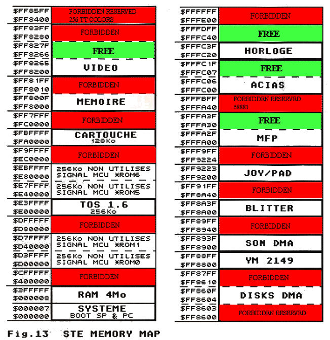
It had a 16-bit data bus, corresponding to data lines D0-D15. This allowed for a 16-bit word to be transferred in a single bus cycle. The UDS and LDS lines addressed either the upper or lower 8 bits of this 16-bit word, allowing for byte-level access. The data lines were read-only.
Beyond address and data lines, several control lines were essential for selecting the ROM and the parts of the data lines to read. These would include the ROM select lines ROM3 and ROM4, as well as UDS and LDS (for upper and lower byte selection).
Bridging Decades: Interfacing the ’80s to 2023
TTL and 5.5V are unmistakably ’80s. In our modern era, we lean towards CMOS technologies, 3.3 volts, and clock speeds in the hundreds of megahertz. Thus, before diving into the selection process for the SidecarTridge Multi-device project’s processing unit, it was glaringly obvious that incorporating a set of level shifters was imperative. These would facilitate conversions between the 5V to 3.3V ranges and from TTL to CMOS technologies—and, of course, back again.
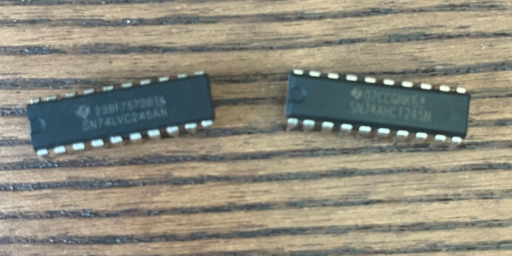
As mentioned earlier, our project involves shifting voltage levels, necessitating different components for optimal compatibility. The conversion from 5 volts to 3.3 volts was managed by leveraging a well-known component: an octal bus transceiver with 3-state outputs, specifically, the Texas Instruments SN74LVC245. This component can be driven by both 3.3-V and 5-V devices, acting as an efficient translator in a mixed 3.3-V/5-V system environment.
The cartridge lines A1-15, UDS, LDS, ROM3, and ROM4 were connected as inputs to it. A crucial feature of this device is the Output-Enabled signal (!OE), allowing for the disabling of the device and effectively isolating the buses. This capability proved pivotal in the final design and was integral to incorporating an RP2040 board.
For converting the output of SidecarT’s processing unit from 3.3 volts to 5 volts, a comparable method was employed, utilizing the Texas Instruments SN74AHCT245. This component, resembling the functionality of the LVC version, facilitates upward voltage translation from 3.3 V to 5 V. Consequently, I leveraged the Output-Enable signal to deactivate the device, isolating the D0-15 data bus lines when not in write mode.
Achieving precise timing for writing data to the bus was critical, as inputting information on the data bus when it wasn’t allocated to the cartridge could result in crashing the Atari ST computer. While the risk isn’t significant when reading the address bus—since it could be regulated by our processing unit—such luxury doesn’t exist on the Atari ST side.
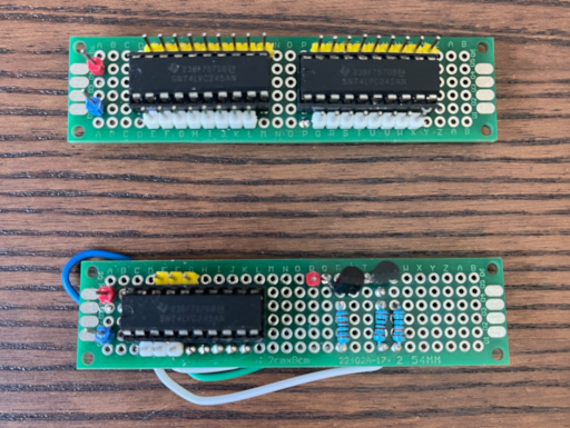
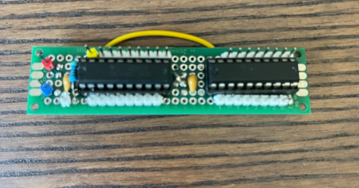
Reusing development boards
To be honest, by this point, I still didn’t know which central processing unit I’d use in the SidecarTridge Multi-device. I knew I had to adapt the type and voltage of the signals, and that’s why I made these cute little development boards to test out different options. While it seemed like a clever idea, the salad of wires was considerable, and my patience was ambushed by my constant worry about the durability of the soldering joints.
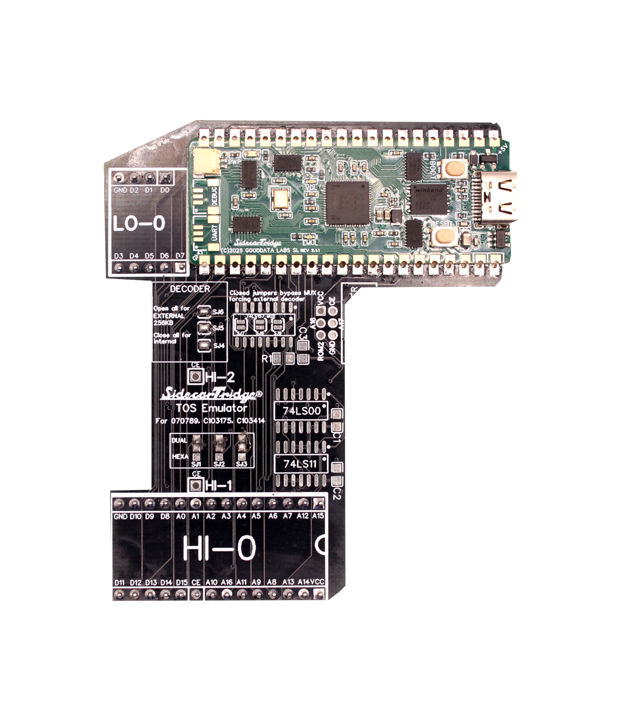
In upcoming blog entries, I’ll spill the beans on choosing the microcontroller RP2040 and compare the mishaps I encountered while scouring for the best possible option. Stay tuned!